Ad Details
-
Ad ID: 43224
-
Added: September 23, 2021
-
Sale Price: ₹ 5000
-
Regular Price: ₹ 5000
-
Condition: Brand New
-
Location: India
-
State: Telangana
-
City: Hyderabad
-
Views: 1754
Description
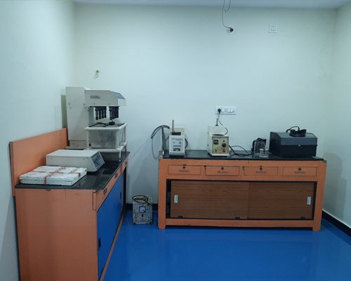
Scanning Electron Microscopy
“Scanning electron microscopy (SEM) is a game-changing technique for the morphological, texture, failure analysis and microstructural composition analysis and the analysis of contaminants present in samples.”
Scanning Electron Microscopy is a test process that produces a magnified image of a sample using an electron beam for analysis. It is highly effective in micro-analysis and failure mode analysis of materials and composites.
SEM analysis can facilitate the analysis of microscopic and nanoscopic materials and objects with great precision. There are two methods of electron detection when using SEM. Backscattered electrons can help with the analysis of the elemental composition of the sample and the secondary electrons emitted close to the surface can reveal relevant information about the topography and morphology of the sample’s surface. Combined with EDX, it can facilitate better analysis of the chemical and elemental composition of the samples.
Our operation of optical microscopes
At our labs and research centers, we make sure to use only the best equipment pieces so that no error can appear in the final results we will provide. Several precautions are maintained so that the sample under consideration does not get damaged during the study.
We ensure that during each new sample test, a sterile and disinfected slide is used for better results. NISHKA professionals ensure that all the arrangement is perfect and no single object is out of the place so that the final data recorded can have the least flaws. The entire material is studied thoroughly with different samples belonging to the same category until the optima studies are obtained.
SEM Applications
SEM testing plays a critical role in the characterization of materials by producing a 2-D High-quality image of the sample. SEM can be used to analyze traits like external morphology, texture, topography and can be used to measure the thickness of the layered structures with the help of cross-sectional imaging. SEM, coupled with EDS, can reveal the chemical composition (Elemental Analysis) of a material. Particulate and contamination analysis gets accelerated by SEM coupled with Energy Dispersive X-ray spectroscopy (EDAX / EDS). It can facilitate and accelerate the investigation and study of interactions between substances and their substrates.
SEM testing is indispensable to mitigate contamination issues, perform failure mode and effects analysis and Identification & characterization of foreign particulates contamination. With the appropriate sampling methods, SEM becomes a powerful tool for an in-depth analysis.
Why NISHKA?
NISHKA’s team of experts has vast experience with in-depth knowledge across various industries such as manufacturing, construction, power, chemicals, medicine and healthcare, electrical, electronics and polymers. This expertise can ensure Total Quality Assurance and can assist in mitigating issues, maintain regulatory standards, and study various materials with ease.
SEM analysis is critical for performing particle composition analysis. The high magnification imaging from our SEM analysis allows clients to understand the wear and tear properties of their material. Our SEM testing services provide analysis of the size, quantity and morphology of small particles. Using these analytical techniques, our team of experts can provide you with valuable insights to best optimize your product cycle.


Leave a Comment
Your email address will not be published. Required fields are marked. *